

The Jinguanming PCBA Solution Development Division mainly collaborates strategically with world-renowned chip manufacturers, specializing in the development of solutions for three major functional areas: optical modules and TYPE C connectors, as well as computer boards and high-speed data transmission function cards.
SMT Assembly Division, under the lean production concept, adapts to the diverse production needs of small batches in the current environment; To achieve high requirements, high quality, and on-time production services;

R&D Process
SMT Prototype Display
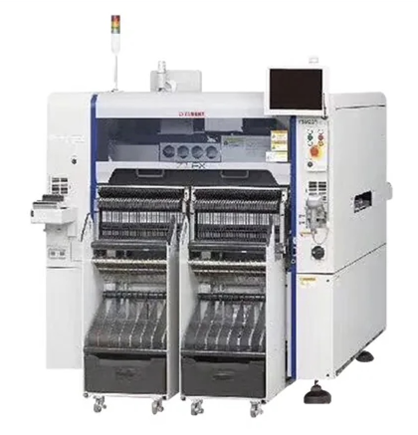
Yamaha YSM20 SMT Machine
Support PCB size: 50 * 50MM-400 * 340MM • SMT accuracy: 0.025mm
Component size: 01005
Maximum supported material types: 318
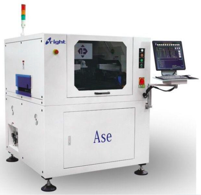
Zhengshi fully automatic printing machine
Minimum size for PCB placement: 400 * 340mm
System alignment accuracy and repeatability accuracy: ± 0.01MM
Actual solder paste printing accuracy: ± 0.025MM
Production Line Configuration
SMT Detection
Standard equipment includes solder paste 3D inspection equipment (SPI) and automatic optical inspection instruments (AOI) before and after reflow oven to ensure printing quality and surface mount quality.
Configure X-ray detector (X-RAY) to analyze chip components, accurately locate and improve defects.
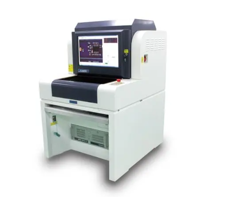
AOI Detector
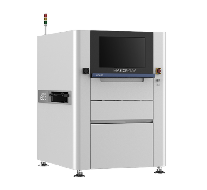
SPI Detector
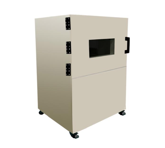
X-ray Detector